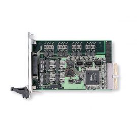
GX5292e Specifications
| Input / Output Channel Features | |
|---|---|
| Logic Families | TTL / LVTTL / CMOS / LVCMOS (1.5 V, 1.8 V, 2.5 V, 3.3 V, or 5 V) , LVDS / LVDM / M-LVDS |
| I/O Levels | TTL / LVTTL / CMOS / LVCMOS: Programmable Output Voltage Level 1.4 V (min); 3.6 V (max) Input Threshold 1.5 V, 1.8 V, 2.5 V, or 3.3 V (5 V tolerant) Recommended Operating Conditions 0 V (min); 5.5 V (max) LVDS / LVDM / M-LVDS: Recommended Operating Conditions Voltage Output: -1.4 V (min); 3.8 V (max) Voltage Input: 0.05 V (min); 3.3 V (max) |
| Channel Timing Skew | 1 ns same card, 1 ns between cards |
| Number of Channels | 32 I/O, direction and configuration is dynamically configurable on a per vector and per channel basis |
| Memory Depth Per Channel | 64 Mb to 2 Gb |
| Test Modes | |
| Stimulus / Response | Drive / Capture daa , up to 64 Mb per channel |
| Timing | |
| Internal Test Clock | |
| Frequency Range | 5 Hz (min); 100 MHz (max) |
| Accuracy | Greater of (±1 Hz or ±0.02% of programmed value) + accuracy of reference clock (PXI 10 MHz or external reference clock) |
| Jitter | ±20 mUI of internal clock frequency, max |
| Reference | PXI 10 MHz or XClk (external clock) input |
| Internal B Clock Output (TTL / LVTTL) | |
| Frequency Range | 300 KHz (min); 100 MHz (max) |
| Accuracy | Greater of (±1 Hz or ±0.5% of programmed value) + accuracy of reference clock |
| Internal C Clock Output (LVDS / LVDM / M-LVDS) | |
| Frequency Range | 3000 KHz (min); 100 MHz (max) |
| Accuracy | Greater of (±1 Hz or ±0.5% of programmed value) + accuracy of reference clock |
| External Test Clock Input | |
| Frequency Range (Configured as Sample Clock) |
0 Hz (min); 100 MHz (max) |
| Frequency Range (Configured as Input to PLL) |
8 MHz (min); 10.5 MHz (max) |
| Pulse Width | 40% (min), 60% (max) |
| Input Level | User selectable I/O level: 1.5 V, 1.8 V, 2.5 V, or 3.3 V (5 V tolerant) |
| External Strobe Clock Input | |
| Frequency Range | 0 Hz (min); 100 MHz (max) |
| Logic Levels | TTL / LVTTL / CMOS / LVCMOS Input Threshold 1.5 V, 1.8 V, 2.5 V, or 3.3 V (5 V tolerant) |
| Power | |
|---|---|
| 3.3 VDC | 200 mA (min); 4 A (max) |
| 12 VDC | 0.03 mA (min); 0.1 mA (max) |
| Environmental | |
| Operating Temperature | 0 °C to +50 °C |
| Storage Temperature | -20 °C to +70 °C |
| Size | 3U PXI |
| Weight | 200 g |
Note: Specifications are subject to change without notice.


