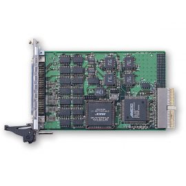
GX3788 Specifications
| Digital I/O Channels | |
|---|---|
| Logic Families | LVTTL, LVDS, configurable for 1.2 / 2.5 / 3.3 V logic; 5 V compatible, programmable per pin via the FPGA |
| Output Current | ±12.0 mA, max. Programmable per pin via the FPGA |
| Input Leakage Current | ±10 µA |
| Power on State | Default is disconnected at power on (unprogrammed FPGA) or defined by FPGA program |
| Number of Channels | 32 Differential Digital I/O lines or 64 Single-ended Digital I/O lines |
| FIFO Depth | 4096 Samples |
| Maximum FIFO Clock Rate | 10 MHz |
| Clock Sources | PXI triggers, Ext Trigger, Star X, PXI Clk10, PXI Clk100 (Express version), DSTAR (Express version), Local bus |
| Protection | Overvoltage: -0.5 V to 7.0 V (input) Short circuit: up to 8 outputs may be shorted at a time |
| Analog Input Channels | |
| Number of Channels | 8 Differential or 16 Single-ended |
| Sample Rate | 1 Hz to 75 kHz Using GX3788AnalogInScanXXX() APIs and channel list |
| Sample Rate Accuracy | 1 Hz to 20 kHz: ±0.5% 20 kHz to 50 kHz: ±1.5% 50 kHz to 75 kHz: ±3.0% |
| Bus Transfer Modes | DMA, Interrupt, Register I/O |
| Resolution | 16-bits |
| Input Voltage Ranges (FS VDC) | ± 13.60 V* ± 10.24 V ± 5.12 V ± 2.56 V ± 1.28 V ± 0.64 V * Uses the gain value for the 10.24 VDC range |
| Input Voltage Accuracy | ± 13.60 V Range: ±7.5 mV ± 10.24 V Range: ±6.5 mV ± 5.12 V Range: ±4.5 mV ± 2.56 V Range: ±4.0 mV ± 1.28 V Range: ±2.0 mV ± 0.64 V Range: ±1.0 mV |
| Input Impedance | 500 M Ohms |
| Analog BW (3 dB) | 8 MHz |
| Over Voltage Protection | ± 24 V |
| CMRR, DC to 60 Hz | 90 dB |
| Channel to Channel Crosstalk | -120 dB (adj. ch.), Fin = 10 kHz |
| Triggering | Trigger in / Trigger out (FPGA controlled) |
| Analog Output Channels | |
|---|---|
| Number of Channels | 8 |
| Conversion Rate | 1 MS/s (simultaneous) |
| Resolution | 16-bits |
| Output Accuracy | ± 6.0 mV |
| Output Range | ± 10 V |
| Output Drive Current | 3 mA |
| Short Circuit Current | 8 mA |
| Output Slew Rate | 6 V/us |
| Timing Sources | |
|---|---|
| PXI Bus | 10 MHz |
| Internal | 80 MHz oscillator, ±20 ppm |
| FPGA and Memory | |
| FPGA Type | Intel/Altera Stratix III, EP3SL50F780 |
| Number of PLLs | 4 |
| Logic Elements | 47.5 K |
| Internal Memory | 1.836 Mb |
| On-Board Memory | 256 K x 32 SSRAM |
| On-Board Flash | 16 MB |
| Power | |
|---|---|
| 3.3 VDC | 3.6 A (typ); 4.9 A (max) |
| 5 VDC | 0.045 A (max) |
| User 3.3 V (@ J1, J2 connector) | 1 A, max |
| User 5 V (@ J3.J4 connector) | 1 A, max |
| Environmental | |
|---|---|
| Operating Temperature | 0 °C to +50 °C |
| Storage Temperature | -20 °C to +70 °C |
| Operational Shock | 30G, ½ sine, 11 ms pulse |
| Vibration (operating) | 2G @ 500 Hz |
| Relative Humidity (operating) | 5% to 80% RH, non-condensing Dew point -5°C – 20°C |
| Relative Humidity (non-operating) | 5% to 95% RH, non-condensing 30°C max |
| Altitude (operating) | Up to 2000 M |
| CE Compliance | EN61010-1 EN61326 |
| Size | 3U PXI |
| Weight | 200 g |
| Calibration Interval | 1 year |
Note: Specifications are subject to change without notice.


