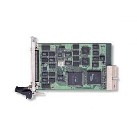
GX3611 Specifications
| GX3500 FPGA Card with GX3511 LVDS Expansion Board | |
|---|---|
| Number of Channels | 80 I/O signals. Direction is configurable by software on a per pin basis |
| Differential Channel Termination | 100 Ω |
| Logic Family | LVDS, compliant with TIA/EIA-644 devices |
| Differential Output Voltage | 247 mV (min); 454 mV (max), Rload = 50Ω |
| Differential Input Voltage Threshold | 50 mV (max), positive going input -50 mV (max), negative going input |
| Absolute Maximum Input Voltage Range | -0.5 V to 4 V |
| Power on State | All channels are configured as inputs |
| Connector | (4) SCSI III, VHDCI type, 68 pin female |
| Timing Sources | |
|---|---|
| PXI Bus | 10 MHz |
| Internal | 80 MHz oscillator, ±20 ppm |
| PCI Clock | 33 MHz |
| FPGA | |
| FPGA Type | Altera Cyclone III, EP3C55 F484 |
| Number of PLLs | Four |
| Logic Elements | 55,856 |
| Internal Memory | 2.34 Mb |
| Power | |
| 3.3 VDC | 2.2 A (max) |
| 5 VDC | 1.2 A (max) |
| Environmental | |
|---|---|
| Operating Temperature | 0 °C to +50 °C |
| Storage Temperature | -20 °C to +70 °C |
| Size | 3U PXI |
| Weight | 200 g |
Note: Specifications are subject to change without notice.


